In addition to Weibo, there is also WeChat
Please pay attention

WeChat public account
Shulou


2026-02-12 Update From: SLTechnology News&Howtos shulou NAV: SLTechnology News&Howtos > Internet Technology >
Share
Shulou(Shulou.com)06/01 Report--
How to use Allegro to turn PCB into 3D, I believe that many inexperienced people do not know what to do. Therefore, this paper summarizes the causes and solutions of the problem. Through this article, I hope you can solve this problem.
As we all know, Cadence is a large-scale EDA software, which can complete almost all aspects of electronic design, including ASIC design, FPGA design and PCB board design. Cadence has absolute advantages in simulation, circuit diagram design, automatic layout and routing, layout design and verification. Most of the tools included in Cadence include almost every aspect of EDA design.
Cadence allegro 16.x version already has 3D view, although it is relatively simple, but in short, it is not bad. In recent years, Cadence is constantly strengthening the three-dimensional display ability of PCB Editor, which can help PCB engineers to design PCB more intuitively. Finally, the arrival of version 17.2 ushered in a new era of Cadence Allegro 3D design, and its 3D effect is no weaker than the 3D View of AD software.
1. Preparation: allegro17.2, 3D model library
2. Setting and display
1. First of all, set up the environment for use.
1) env file settings. The path is at: CadenceSPB_16.6sharepcbte xtenv, open to see if set step_unsupported_prototype 1 is set, and if not, add it to the file.
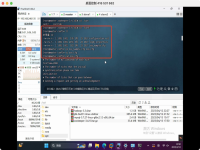
2) Step model path setting. The following figure is shown:
2. Set the matching between the components in PCB and 3D model
1) enter the matching interface.
2) match settings
In the position shown above, the devices that need to display 3D effect are selected to match, and the parameters are set to achieve the ideal effect. Click Save to save it after setting it up. You can then click Report to view the matching results.
3. Display settings.
1) the corresponding layer must be opened before display.
PACKAGE GEOMETRY/PLACE_BOUND_TOP
PACKAGE GEOMETRY/PLACE_BOUND_BOTTOM
MANUFACTURING/STEP3D_ASSEMBLY_ENCLOSURE
2) set 3D to display the viewing effect.
To this step, beautiful 3D has been made, is not very beautiful, then you also have a try!
After reading the above, have you mastered how to use Allegro to turn PCB into 3D? If you want to learn more skills or want to know more about it, you are welcome to follow the industry information channel, thank you for reading!
Welcome to subscribe "Shulou Technology Information " to get latest news, interesting things and hot topics in the IT industry, and controls the hottest and latest Internet news, technology news and IT industry trends.
Views: 0
*The comments in the above article only represent the author's personal views and do not represent the views and positions of this website. If you have more insights, please feel free to contribute and share.

The market share of Chrome browser on the desktop has exceeded 70%, and users are complaining about

The world's first 2nm mobile chip: Samsung Exynos 2600 is ready for mass production.According to a r


A US federal judge has ruled that Google can keep its Chrome browser, but it will be prohibited from

Continue with the installation of the previous hadoop.First, install zookooper1. Decompress zookoope


About us Contact us Product review car news thenatureplanet
More Form oMedia: AutoTimes. Bestcoffee. SL News. Jarebook. Coffee Hunters. Sundaily. Modezone. NNB. Coffee. Game News. FrontStreet. GGAMEN
© 2024 shulou.com SLNews company. All rights reserved.