In addition to Weibo, there is also WeChat
Please pay attention

WeChat public account
Shulou


2026-02-07 Update From: SLTechnology News&Howtos shulou NAV: SLTechnology News&Howtos > IT Information >
Share
Shulou(Shulou.com)11/24 Report--
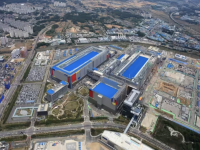
Thanks to CTOnews.com netizen OC_Formula for the clue delivery! CTOnews.com, Oct. 2-Intel said last week that it had begun mass production using EUV lithography at its $18.5 billion Irish plant, calling it a "milestone moment."
Ann Kelleher, general manager of Intel technology development, said Intel would take the lead in introducing the next generation of high numerical aperture (High-NA) EUV lithography machines this year, after Intel had said that High-NA technology would be used only for device development and verification on 18A nodes and would be officially put into production on nodes after 18A.
The US company said that with the High-NA EUV lithography machine, it could theoretically play a key role in Intel's realization of its "four-year and five-generation process".
Ankelleher said that they are currently achieving this goal as planned, with two manufacturing processes completed, while the third process is "coming quickly" and that the last two processes have made very good progress.
Peter Wennink, chief executive of Tuyuan PixabayASML, told Reuters last month that despite some obstacles from suppliers, the company would deliver the High NA EUV machine by the end of the year as previously planned.
Intel expects to receive the first High-NA EUV lithography machines in Oregon later this year, and Intel will be the first chipmaker to acquire the machine, Mr. Kelleher said.
ASML said that a High-NA EUV device the size of a truck, each worth more than $150 million (CTOnews.com Note: currently about 1.095 billion yuan), can meet the needs of all kinds of chipmakers and can make smaller, more advanced chips in the next decade.
At present, the most advanced chip is the 4amp 5nm process, and Samsung and TSMC can also mass produce 3nm technology in the second half of the year. For Twinscan NXE:3400C and similar systems using ASML EUV lithography technology, most of them have 0.33 NA (numerical aperture) optical devices that can provide 13 nm resolution.
At present, this resolution size is sufficient for single modes of 7 nm / 6 nm nodes (36 nm ~ 38 nm) and 5nm (30 nm ~ 32 nm). However, with the arrival of a distance of less than 30 nm (more than 5nm nodes), a 13 nm resolution may require double exposure, which is the mainstream method in the next few years.
For the post-3nm era, ASML and its partners are developing a new EUV lithography machine, the Twinscan EXE:5000 series, which will have a 0.55 NA (high NA) lens with a resolution of up to 8nm, minimizing processes, reducing costs and providing yield in 3nm and above nodes.
Welcome to subscribe "Shulou Technology Information " to get latest news, interesting things and hot topics in the IT industry, and controls the hottest and latest Internet news, technology news and IT industry trends.
Views: 0
*The comments in the above article only represent the author's personal views and do not represent the views and positions of this website. If you have more insights, please feel free to contribute and share.

The market share of Chrome browser on the desktop has exceeded 70%, and users are complaining about

The world's first 2nm mobile chip: Samsung Exynos 2600 is ready for mass production.According to a r


A US federal judge has ruled that Google can keep its Chrome browser, but it will be prohibited from

Continue with the installation of the previous hadoop.First, install zookooper1. Decompress zookoope


About us Contact us Product review car news thenatureplanet
More Form oMedia: AutoTimes. Bestcoffee. SL News. Jarebook. Coffee Hunters. Sundaily. Modezone. NNB. Coffee. Game News. FrontStreet. GGAMEN
© 2024 shulou.com SLNews company. All rights reserved.