In addition to Weibo, there is also WeChat
Please pay attention

WeChat public account
Shulou


2026-02-14 Update From: SLTechnology News&Howtos shulou NAV: SLTechnology News&Howtos > IT Information >
Share
Shulou(Shulou.com)11/24 Report--
Thanks to CTOnews.com netizen OC_Formula for the clue delivery! CTOnews.com, May 8, 2023 International Symposium on VLSI Technology will be held in Kyoto, Japan from June 11 to 16. Officials have now revealed in advance some of the things that will be revealed at the summit.
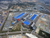
In addition to technical demonstrations, VLSI seminars will include demonstration sessions, joint focus meetings, evening group discussions, short courses, seminars and special forums. At that time, there will also be some key papers on CMOS technology at the forefront of science and technology, such as "the world's first GAA 3nm process using new MBCFET technology (SF3)".
Samsung 3nm technology is so highly anticipated because it enables the transition from FinFET to Gate-All-Around transistor architecture. It is said that compared with the 4nm FinFET platform, SF3 has achieved 22% frequency increase, 34% energy efficiency improvement and 21% area reduction (PPA).
Samsung SF3 technology is the industry's first mass production GAA process upgrade, using multi-bridge channel MBCFET (Multi-Bridge-Channel FET) design, can provide a variety of nano-wafer width to provide a fairly good performance, at a fixed standard cell height significantly improve the chip-level power performance matrix, thus surpassing the FinFET platform.
According to South Korean media, Samsung will focus on 3nm production in 2023-2024, namely SF3 (3GAP) and its improved version SF3P (3GAP+). Its production yield can be maintained in the initial range of 60-70%, and the company plans to launch its 2-nm nodes in 2025-2026.
After Samsung and TSMC have entered the era of 3nm process, 3nm process will become the mainstream of wafer foundry market in the future. As a result, the 3nm process market is expected to be worth as much as $25.5 billion by 2025 (CTOnews.com Note: currently about 176.205 billion yuan), surpassing the $19.3 billion estimated at the time of 5nm.
In the third quarter of 2022, TSMC still ranks first in the global wafer foundry market with a market share of 53.4%, while Samsung, which ranks second, has a market share of 16.4%, according to TrendForce, a market research firm based on Tu Yuan Unsplash. Therefore, in the fierce competition in the market, the 3nm process will become the key to the main competition between the two companies in the future.
Welcome to subscribe "Shulou Technology Information " to get latest news, interesting things and hot topics in the IT industry, and controls the hottest and latest Internet news, technology news and IT industry trends.
Views: 0
*The comments in the above article only represent the author's personal views and do not represent the views and positions of this website. If you have more insights, please feel free to contribute and share.

The market share of Chrome browser on the desktop has exceeded 70%, and users are complaining about

The world's first 2nm mobile chip: Samsung Exynos 2600 is ready for mass production.According to a r


A US federal judge has ruled that Google can keep its Chrome browser, but it will be prohibited from

Continue with the installation of the previous hadoop.First, install zookooper1. Decompress zookoope


About us Contact us Product review car news thenatureplanet
More Form oMedia: AutoTimes. Bestcoffee. SL News. Jarebook. Coffee Hunters. Sundaily. Modezone. NNB. Coffee. Game News. FrontStreet. GGAMEN
© 2024 shulou.com SLNews company. All rights reserved.