In addition to Weibo, there is also WeChat
Please pay attention

WeChat public account
Shulou


2026-02-12 Update From: SLTechnology News&Howtos shulou NAV: SLTechnology News&Howtos > IT Information >
Share
Shulou(Shulou.com)11/24 Report--
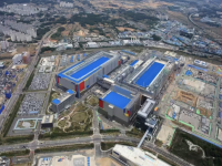
Thanks to CTOnews.com netizen OC_Formula for the clue delivery! CTOnews.com, April 16, Samsung Electronics launched a 4-nanometer multi-project wafer (MPW) service for the first time this month, proving the stabilization of yield. In the four years since the launch of the MPW 5 nano process in 2019, Samsung has achieved finer and more advanced processes along the way.
▲ source: Samsung Electronics industry insiders said on the 14th that Samsung Electronics plans to launch the 4nm MPW service for the first time this month. CTOnews.com found that Samsung Electronics marked 4 Nano Engineering as SF4, and they plan to conduct two more MPW in August and December.
MPW services are technologies that make multiple semiconductors on a single wafer. Before a fab company releases its chip, it has to stream the chip through the foundry (production line), that is, the MPW process of the chip prototype. If its customers get the first samples and sign an order, the foundry will start mass production, and the more MPW services there are, the more opportunities for fabless companies to produce chip prototypes.
An industry source explained, "the 4-nanometer process MPW means that we have ensured that the yield is stable to support prototype production."
To put it simply, since MPW is a process for fabless companies to prototype chips prior to product release, the service can only be started after meeting conditions such as yield and speed and reducing TAT (turnaround time, time from receipt of order to delivery). Therefore, Samsung Electronics' launch of 4nm MPW is interpreted as a performance that the yield is stable and will expand the scale of mass production.
Last October, Jung Ki-tae, vice president of technical development of Samsung Electronics wafer foundry division, said at Samsung Foundry Forum 2022 at COEX, "the initial yield of 4nm failed to meet market expectations, but now we have reached a level where we expect the yield to exceed that of the previous generation. I believe there will be no capacity problems in the future."
People in the system semiconductor industry said: "MPW is different even for semiconductors of the same process and size, so it is difficult to price uniformly." generally speaking, the cost of IP is higher than the cost of a fab. 4nm and 5nm process MPW is an expensive process that costs billions of won. "
Welcome to subscribe "Shulou Technology Information " to get latest news, interesting things and hot topics in the IT industry, and controls the hottest and latest Internet news, technology news and IT industry trends.
Views: 0
*The comments in the above article only represent the author's personal views and do not represent the views and positions of this website. If you have more insights, please feel free to contribute and share.

The market share of Chrome browser on the desktop has exceeded 70%, and users are complaining about

The world's first 2nm mobile chip: Samsung Exynos 2600 is ready for mass production.According to a r


A US federal judge has ruled that Google can keep its Chrome browser, but it will be prohibited from

Continue with the installation of the previous hadoop.First, install zookooper1. Decompress zookoope


About us Contact us Product review car news thenatureplanet
More Form oMedia: AutoTimes. Bestcoffee. SL News. Jarebook. Coffee Hunters. Sundaily. Modezone. NNB. Coffee. Game News. FrontStreet. GGAMEN
© 2024 shulou.com SLNews company. All rights reserved.