In addition to Weibo, there is also WeChat
Please pay attention

WeChat public account
Shulou


2026-02-15 Update From: SLTechnology News&Howtos shulou NAV: SLTechnology News&Howtos > IT Information >
Share
Shulou(Shulou.com)11/24 Report--
Thanks to CTOnews.com netizens Wu Yanzu in South China for the delivery of clues! CTOnews.com March 22, Nvidia has worked with TSMC, ASML and Synopsys. After four years of development, Nvidia has finally completed the new AI acceleration technology cuLitho. According to reports, CuLitho can increase the computing optical scale of the next generation of chips by more than 40 times, making it possible to manufacture 2nm and more advanced chips.
CuLitho is an operational microshadow function library that will shorten the mask duration of advanced process chips, improve the yield, and greatly reduce the energy consumption required for wafer fabrication.
According to Taiwan's United Daily News, TSMC will certify the production of cuLitho in June this year and complete the trial production of 2nm, which will be used to improve the yield of the 2nm process and shorten the mass production schedule.
According to reports, the new NVIDIA cuLitho software library for computational lithography has been integrated by TSMC and Xinsi Technology into its latest generation of NVIDIA Hopper architecture GPU software, manufacturing processes and systems, while the equipment manufacturer ASML cooperates closely with NVIDIA in GPU and cuLitho, and plans to integrate GPU support into all its computational lithography software products.
NVIDIA Huang Renxun said, "the chip industry is the foundation of almost every other industry in the world, and as lithography technology reaches its physical limits, NVIDIA has launched cuLitho and partnered with our partners TSMC, ASML and Synopsys to enable fabs to increase production, reduce their carbon footprint and lay the foundation for 2nm and higher processes."
Nvidia says cuLitho can bring a 40-fold performance leap compared to current lithography-the process of etching patterns on silicon wafers-much faster than large-scale computing that "consumes tens of billions of CPU hours a year".
It is reported that it can use 500 NVIDIA DGX H100 systems to achieve what could have been done by 40000 CPU systems, running all parts of the lithography process in parallel, thus helping to reduce power demand and potential environmental impact.
"Computational lithography is the largest computing workload in chip design and manufacturing, consuming tens of billions of CPU hours a year. 24x7, a large data center, operates around the clock to create masks for lithography systems. These data centers are part of the nearly $200 billion capital expenditure that chipmakers invest annually." Huang Renxun said that cuLitho can increase the speed of computational lithography to 40 times. For example, the Nvidia H100 GPU requires 89 masks to make, and it takes two weeks to process a single mask when running on the CPU, while it only takes eight hours to run cuLitho on the GPU.
It is reported that TSMC can reduce power from 35MW to 5MW by using cuLitho acceleration on 500 DGX H100 systems, replacing the 40000 CPU servers previously used for computing lithography. Wafer factories that use cuLitho can produce 3-5 times more masks (Mask, also known as mask, that is, templates for chip design) per day, but only need 1max 9 of the current power configuration.
Of course, the cuLitho accelerator library is also compatible with Ampere and Volta GPU, but Hopper is by far the fastest solution.
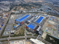
According to previous reports by CTOnews.com, TSMC's construction of a Fab20 super-large wafer plant in Zhuke Baoshan Phase II will be used as a 2nm production base and become a major town of 2nm. The first phase of the Fab20 plant is expected to start risk trial production in 2024 and mass production in 2025, while the second phase is currently under construction and is expected to gradually enter risk trial production and mass production after the first phase.
According to the cooperative plan of four major semiconductor companies, the progress in this technology will make it possible to use finer circuits on the chip, speed up time to market, and improve the energy efficiency of large-scale data centers that operate throughout the day to promote the manufacturing process.
Wei Zhijia, president of TSMC, said that the cuLitho team handed over the time-consuming work to GPU to carry out, and made significant progress in speeding up the expression Weiying technology. This development makes it possible for TSMC to deploy Weiying technology solutions such as reverse Weiying technology and deep learning in chip manufacturing, and provides an important contribution to the continuity of semiconductor miniaturization.
Welcome to subscribe "Shulou Technology Information " to get latest news, interesting things and hot topics in the IT industry, and controls the hottest and latest Internet news, technology news and IT industry trends.
Views: 0
*The comments in the above article only represent the author's personal views and do not represent the views and positions of this website. If you have more insights, please feel free to contribute and share.

The market share of Chrome browser on the desktop has exceeded 70%, and users are complaining about

The world's first 2nm mobile chip: Samsung Exynos 2600 is ready for mass production.According to a r


A US federal judge has ruled that Google can keep its Chrome browser, but it will be prohibited from

Continue with the installation of the previous hadoop.First, install zookooper1. Decompress zookoope


About us Contact us Product review car news thenatureplanet
More Form oMedia: AutoTimes. Bestcoffee. SL News. Jarebook. Coffee Hunters. Sundaily. Modezone. NNB. Coffee. Game News. FrontStreet. GGAMEN
© 2024 shulou.com SLNews company. All rights reserved.