In addition to Weibo, there is also WeChat
Please pay attention

WeChat public account
Shulou


2026-02-11 Update From: SLTechnology News&Howtos shulou NAV: SLTechnology News&Howtos > Internet Technology >
Share
Shulou(Shulou.com)06/02 Report--
This article mainly introduces "what is the difference between Plane and Layer in PCB". In daily operation, I believe that many people have doubts about the difference between Plane and Layer in PCB. The editor consulted all kinds of materials and sorted out simple and easy-to-use methods of operation. I hope it will be helpful to answer the question of "what is the difference between Plane and Layer in PCB?" Next, please follow the editor to study!
When designing PCBLayout, according to the needs of the project, to design multi-tier PCB, you need to add "layers". Take Altium Designer as an example, the layers to be added can be divided into "Plane" and "Player". So what's the difference between Plane and Player?
Layer for the front, in this layer, to draw a line is to draw a wire, that is, wherever the line is drawn, there is a copper connection. Plane is negative, that is, the so-called "negative film method", this layer itself is a piece of copper skin, draw a line, is to separate the copper skin, that is, wherever the line is to remove the copper skin.

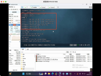
When adding layers, the options for adding layers can be divided into "Layer" and "Plane", as shown in ↑ above.

Press the shortcut L on Altium Designer and you can see that Layer is on the side of Signal Layers and Plane is on the side of Internal Planes, as shown in ↑ above.
In the Plane layer, there are many through holes with a cross mark, indicating that the through hole is connected to the layer, such as ↑ above.
Such as the Plane of ↑ above, the wiring divides this layer into four areas, each of which can be added with a network label that needs to be connected, which is also called "internal electrical layer division".
Such as the picture above ↑, this layer is Layer, wiring is the wire. At this point, the study on "what is the difference between Plane and Layer in PCB" is over. I hope to be able to solve your doubts. The collocation of theory and practice can better help you learn, go and try it! If you want to continue to learn more related knowledge, please continue to follow the website, the editor will continue to work hard to bring you more practical articles!
Welcome to subscribe "Shulou Technology Information " to get latest news, interesting things and hot topics in the IT industry, and controls the hottest and latest Internet news, technology news and IT industry trends.
Views: 0
*The comments in the above article only represent the author's personal views and do not represent the views and positions of this website. If you have more insights, please feel free to contribute and share.

The market share of Chrome browser on the desktop has exceeded 70%, and users are complaining about

The world's first 2nm mobile chip: Samsung Exynos 2600 is ready for mass production.According to a r


A US federal judge has ruled that Google can keep its Chrome browser, but it will be prohibited from

Continue with the installation of the previous hadoop.First, install zookooper1. Decompress zookoope


About us Contact us Product review car news thenatureplanet
More Form oMedia: AutoTimes. Bestcoffee. SL News. Jarebook. Coffee Hunters. Sundaily. Modezone. NNB. Coffee. Game News. FrontStreet. GGAMEN
© 2024 shulou.com SLNews company. All rights reserved.